Whether you're tinkering with DIY projects or crafting sophisticated electronic devices, mastering PCB design is essential for turning concepts into reality.
the intricate world of PCB design training in Bangalore, equipping you with the knowledge to navigate complexities and unleash your creativity.
Understanding PCB Design Fundamentals
At the core of PCB design lies a fundamental understanding of its components and functionalities. A PCB serves as a platform for connecting electronic components through conductive pathways, facilitating seamless interaction between different elements of a circuit. By comprehending the basics of circuitry, including voltage, current, resistance, and capacitance, you lay the groundwork for efficient PCB design.
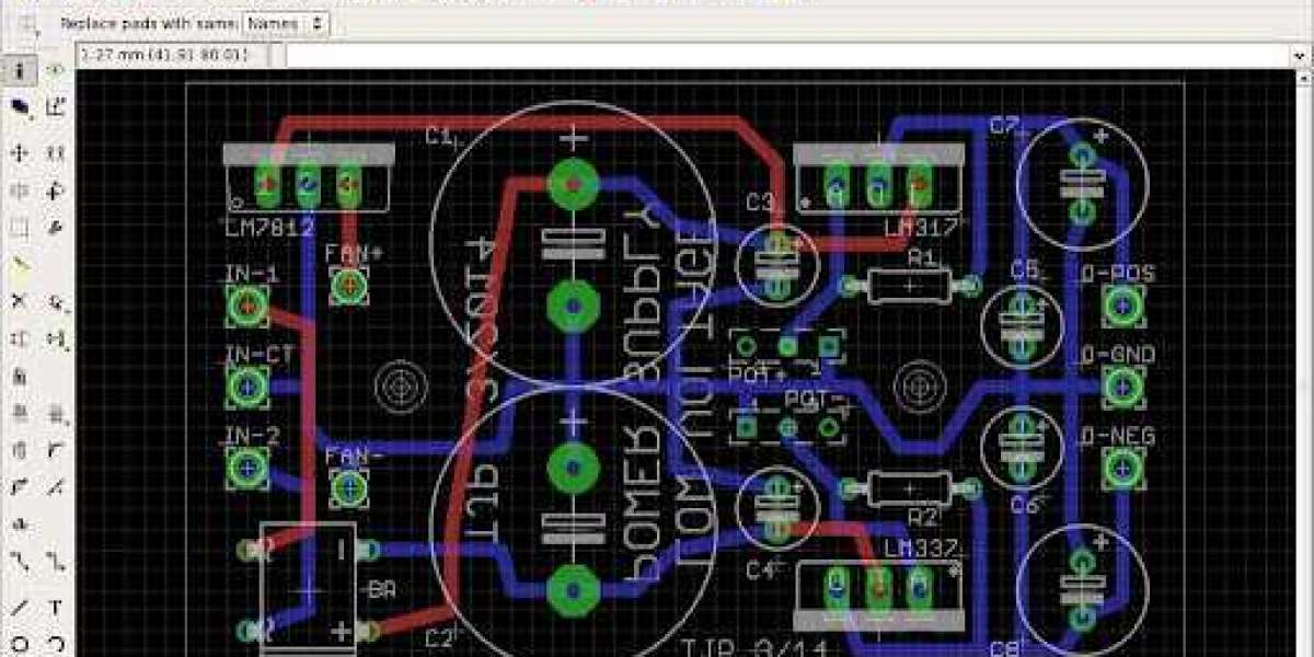
Exploring PCB Design Software
In the digital age, harnessing the power of PCB design software is paramount. Advanced tools such as Altium Designer, Eagle, and KiCad empower engineers and enthusiasts alike to translate conceptual designs into tangible PCB layouts. These software solutions offer a plethora of features, including schematic capture, component libraries, and simulation capabilities, streamlining the design process and fostering innovation.
mermaid
Copy code
graph TD;
A[Conceptual Design] -- B(Schematic Capture);
B -- C(Component Placement);
C -- D(Routing);
D -- E(Verification);
E -- F(Fabrication);
Optimizing PCB Layouts for Performance and Efficiency
Efficient PCB layout is the cornerstone of reliable electronic systems. By strategically placing components, minimizing signal interference, and optimizing trace routing, designers can enhance performance while minimizing manufacturing costs. Factors such as signal integrity, thermal management, and electromagnetic compatibility (EMC) play pivotal roles in determining the success of a PCB layout.
Leveraging Advanced PCB Design Techniques
Innovation thrives on the integration of advanced PCB design techniques. From multilayer PCBs to high-speed signal routing, embracing cutting-edge methodologies enables designers to push the boundaries of what's possible. Techniques such as impedance matching, differential signaling, and signal integrity analysis empower engineers to design robust PCBs capable of meeting the demands of modern electronics.
Ensuring Design Integrity through Prototyping and Testing
Prototyping and testing are integral phases in the PCB design process, serving as litmus tests for design integrity and functionality. Rapid prototyping techniques, such as 3D printing and CNC milling, allow designers to quickly iterate and refine their designs before mass production. Additionally, thorough testing procedures, including functional testing, environmental testing, and reliability testing, ensure that PCBs meet stringent quality standards.
Embracing Industry Best Practices and Standards
Adhering to industry best practices and standards is imperative for achieving success in PCB design. Standards such as IPC-A-600 for Acceptability of Printed Boards and IPC-2221 for Generic Standard on Printed Board Design provide guidelines for design, manufacturing, and assembly processes. By aligning with these standards, designers can enhance compatibility, reliability, and manufacturability of their PCB designs.